Mufeng Chen
Cross-Layer Heterogeneous Memory Systems for AI and Optimization. Ph.D. student, ECE, Purdue University · NanoX Lab.

West Lafayette, IN, USA
chen5240 [at] purdue.edu
I am a Ph.D. student in Electrical and Computer Engineering at Purdue University, advised by Prof. Haitong Li in the NanoX Lab. My current research focuses on GPU and heterogeneous memory-system architecture for AI and LLM workloads, within the broader theme of cross-layer heterogeneous memory systems for AI and optimization.
Research areas
I study how memory-hierarchy design and data movement shape the efficiency of AI and LLM systems. My ongoing work explores high-bandwidth flash within heterogeneous memory systems for GPU-based AI workloads. At the cache level, my GPU architecture project explores register-file caching and warp scheduling.
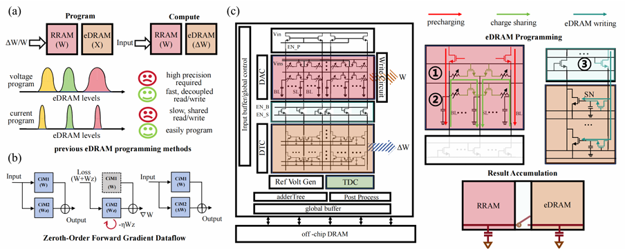
This systems focus builds on my research in memory technologies and circuit–architecture co-design. At the domain-specific accelerator level, my published work includes my first-author paper on analog multilevel eDRAM–RRAM CIM for LLM fine-tuning, the CENTAUR floating-point CIM engine, the PROTEUS programmable CIM accelerator, and heterogeneous CIM fabrics for edge inference and learning. Explore the research overview.
Before Purdue, I conducted research at Zhejiang University under Prof. Er-Ping Li. I completed summer research internships at Rice University’s SIMS Lab with Prof. Kaiyuan Yang in 2022 and Purdue’s NanoX Lab with Prof. Haitong Li in 2023. I earned a B.Eng. in Optical and Electronic Information Engineering from Huazhong University of Science and Technology.
news
| Aug 01, 2026 | PROTEUS, our 40 nm programmable general-purpose digital CiM accelerator, is available in early access at IEEE JSSC. [paper] |
|---|---|
| Apr 01, 2026 | Presented Heterogeneous Compute-in-Memory Fabrics for Efficient, Scalable Edge Inference and Learning at ISQED 2026. [paper] |
| Nov 01, 2025 | CENTAUR, a 38.5-TFLOPS/W floating-point digital CiM engine, presented at IEEE A-SSCC 2025. [paper] |
| May 21, 2025 | Presented Analog Multilevel eDRAM-RRAM CIM for Zeroth-Order Fine-tuning of LLMs at IEEE IMW 2025 in Monterey, CA. [paper] |
| Aug 19, 2024 | Started my Ph.D. in Electrical and Computer Engineering at Purdue University, joining the NanoX Lab. |